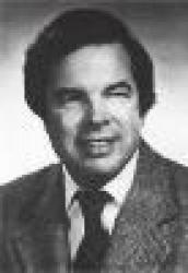
Walter Brattayn
 USA
USA- Biography of Walter Houser Brattain
- Early Career
- Transistor Discovery
- Transistor Effect
- Field-Effect Transistors
- Nobel Prize and Later Life
Biography of Walter Houser Brattain
Walter Houser Brattain was an American physicist who, along with John Bardeen, discovered the transistor effect in 1948 and created the first transistor. He was born in Amoy (Xiamen), China, to Ross R. Brattain, a teacher at a private school for Chinese children, and Ottilie (Houser) Brattain. He was the eldest of five children. Brattain's family returned to the state of Washington in the early years of his childhood and settled in Tonasket. His father purchased land, becoming the owner of a cattle ranch and a mill. Brattain attended school in Tonasket and later enrolled at Whitman College in Walla Walla, where he studied mathematics and physics. He earned a Bachelor's degree in 1924, a Master's degree in Physics from the University of Oregon in 1926, and a Ph.D. in Physics from the University of Minnesota in 1929. Despite enjoying life on the ranch and in nature, Brattain despised farming work. He once said, "Being dragged around in the dust behind three horses and a plow is what made me a physicist."
Early Career
In his first seven years at Bell Labs, Brattain studied phenomena such as the influence of adsorption films on electron emission from hot surfaces, electron collisions in mercury vapor, and worked on magnetometers, infrared phenomena, and frequency standards. At that time, the main electronic amplifying device was the vacuum tube triode, invented by Lee De Forest in 1907. Thomas Edison had discovered that an electric current could be produced between a heated filament and a second electrode placed in a hermetically sealed bulb when the air was evacuated and a battery connected. This led to the invention of the two-electrode vacuum tube diode. Physicists later showed that the filament emitted electrons, which carried a negative charge and were attracted to the positive electrode. Since diodes only conduct current in one direction, they were used as rectifiers to convert alternating current into direct current flowing in only one direction. De Forest inserted a wire mesh (grid) between the electron emitter (cathode) and the positive electrode (anode). A small change in voltage on the grid led to large changes in the current flowing through the grid between the cathode and anode, allowing the amplification of a signal applied to the grid. The high temperature required for electron emission shortened the cathode's lifespan and degraded the electronic tube. Brattain discovered that certain thin cathode coatings provided satisfactory emission at lower temperatures, enhancing the effect and extending the tube's lifespan.
Transistor Discovery
When William Shockley joined Bell Labs in 1936, he quickly became involved in studying the properties of materials called semiconductors. His goal was to replace vacuum electronic tubes with solid-state devices that would be smaller, less fragile, and more energy-efficient. The electrical conductivity of semiconductors is intermediate between that of conductors (mainly metals) and insulators and changes significantly even with small amounts of impurities. The first semiconductor radios used a contact between a thin wire (whisker) and a piece of galena mineral (semiconductor) to detect weak signals from received radio waves. While studying semiconductors, Brattain and Shockley searched for a material that could both detect and amplify signals. Their research was interrupted by World War II, and from 1942 to 1945, they worked in the war research division at Columbia University, applying scientific developments to anti-submarine warfare. Shockley left the research even earlier to work on radar. When Brattain and Shockley returned to Bell Labs after the war, they were joined by theoretical physicist John Bardeen. In this collaboration, Brattain served as the experimentalist, determining the properties and behavior of the materials and devices under investigation. Shockley proposed the theoretical idea that by applying an electric field to the current, it was possible to create a field-effect amplifier. This field would act similarly to the field that arises on the grid of a triode amplifier. The group created many devices to test Shockley's theory but with no success.
Transistor Effect
It was then that Bardeen had the thought that the field could not penetrate inside the semiconductor due to the layer of electrons on its surface. This led to intensive research on surface effects. The surfaces of semiconductors were subjected to light, heat, cold, wetting with liquids (insulating and conducting), and covered with metal films. In 1947, after the group delved deeply into the behavior of semiconductor surfaces, Brattain and Bardeen constructed a device in which the transistor effect, later known as the point-contact transistor, first manifested itself. This device consisted of a germanium crystal containing a small concentration of impurities. On one side of the crystal, there were two contacts made of gold foil, and on the other side, there was a third contact. Positive voltage was applied between the first gold contact (emitter) and the third contact (base), and negative voltage was applied between the second gold contact (collector) and the base. The signal applied to the emitter influenced the current in the collector-base circuit. Although this device amplified the signal as intended, the principle of its operation remained unexplained, leading to further research. While the theory of semiconductors had already been developed to a large extent through quantum mechanics, the predictions of this theory had not yet found adequate quantitative confirmation in experiments. Atoms in crystals are held together by electrons weakly bound to their nuclei. In a perfect crystal, the bonds are "saturated" or "filled." Electrons are difficult to detach, and they move with difficulty, leading to very high electrical resistance. Such a crystal is an insulator. However, the inclusion of foreign atoms that do not perfectly fit into the crystal structure leads to either the appearance of excess electrons capable of participating in electric current or a deficit of electrons known as "holes." In the mathematical model, the holes move as if they were positively charged electrons, albeit at a different speed. In fact, holes are vacancies left by electrons, and therefore, everything appears as if holes move in the opposite direction while electrons move in the forward direction, filling previously empty places and creating new holes where they left. It was found that explaining the action of the transistor required considering the complex interaction of different types and concentrations of impurities, the local character of contacts between different materials, and the contribution that both electrons and holes give to the current. The important role of holes was not adequately anticipated in advance.
Field-Effect Transistors
Shockley predicted that the device could be improved by replacing metal-semiconductor contacts with higher-quality contacts between different types of semiconductors, one dominated by excess electrons (n-type) and the other by holes (p-type). A successful model called the junction transistor was made in 1950. It consisted of a thin layer of the p-type sandwiched between two layers of n-type with metallic contacts in each layer. This device worked exactly as Shockley had predicted. Junction transistors quickly replaced point-contact types as they were easier to manufacture and performed better. Shockley's early idea of a field-effect transistor had been difficult to realize because suitable materials were not available. Working field-effect transistors were only constructed using silicon crystals when crystal growth and purification methods had significantly advanced. Similar to electron tubes, transistors allow a small current flowing in one circuit to control a much larger current flowing in another circuit. Transistors quickly replaced radio tubes everywhere except in cases where it is necessary to control very high power, such as in broadcasting or industrial radio frequency heating installations. Bipolar transistors are usually used where high speed is required, as well as in high-frequency applications where it is not necessary to use electronic tubes. Field-effect transistors are the main type of transistors used in electronic devices. They are easier to manufacture and consume even less energy than bipolar transistors. Although some transistors are still made from germanium, the majority are made from silicon, which is more resistant to high temperatures. With further technological advancements, it became possible to fit up to a million transistors in a single silicon chip, and the number continues to increase. These silicon blocks serve as the foundation for the rapid development of modern computers, communication devices, and control systems.
Nobel Prize and Later Life
Brattain, Bardeen, and Shockley shared the Nobel Prize in Physics in 1956 "for their researches on semiconductors and their discovery of the transistor effect." In his Nobel lecture titled "Surface Properties of Semiconductors," Brattain emphasized the importance of surfaces, where "many, if not the majority, of interesting and useful phenomena occur. In electronics, most, if not all, circuit elements involve out-of-equilibrium phenomena that occur on surfaces." Brattain's further research on the properties of semiconductors and their surfaces was crucial for field-effect transistors, which are highly sensitive to surface defects, and for solar cells, whose properties are determined by the electrical properties of the surface.
In 1935, Brattain married Keren Gilmore, who was involved in physical chemistry, and they had a son. She passed away in 1957, and a year later, Brattain married Emma Jane Kirsch Miller. Known for his direct and sincere nature, Brattain enjoyed hobbies such as golfing, fishing, and reading books. Among his other awards, Brattain received the Stuart Ballantine Medal from the Franklin Institute (1952), the John Scott Medal from the City of Philadelphia (1955), and an honorary degree from the University of Oregon (1976). He holds five honorary doctorates, is a member of the National Academy of Sciences and the Inventors Hall of Fame, and is also a fellow of the American Academy of Arts and Sciences, the American Association for the Advancement of Science, and the American Physical Society.